- 您现在的位置:买卖IC网 > Sheet目录364 > SST49LF008A-33-4C-EIE-T (Microchip Technology)IC FLASH FWH 8MBIT 33MHZ 40TSOP
�� �
�
�8� Mbit� Firmware� Hub�
�A� Microchip� Technology� Company�
�SST49LF008A�
�Data� Sheet�
�Design� Considerations�
�SST� recommends� a� high� frequency� 0.1� μF� ceramic� capacitor� to� be� placed� as� close� as� possible�
�between� V� DD� and� V� SS� less� than� 1� cm� away� from� the� V� DD� pin� of� the� device.� Additionally,� a� low� fre-�
�quency� 4.7� μF� electrolytic� capacitor� from� V� DD� to� V� SS� should� be� placed� within� 1� cm� of� the� V� DD� pin.� If� you�
�use� a� socket� for� programming� purposes� add� an� additional� 1-10� μF� next� to� each� socket.�
�The� RST#� pin� must� remain� stable� at� V� IH� for� the� entire� duration� of� an� Erase� operation.� WP#� must�
�remain� stable� at� V� IH� for� the� entire� duration� of� the� Erase� and� Program� operations� for� non-Boot� Block�
�sectors.� To� write� data� to� the� top� Boot� Block� sectors,� the� TBL#� pin� must� also� remain� stable� at� V� IH� for� the�
�entire� duration� of� the� Erase� and� Program� operations.�
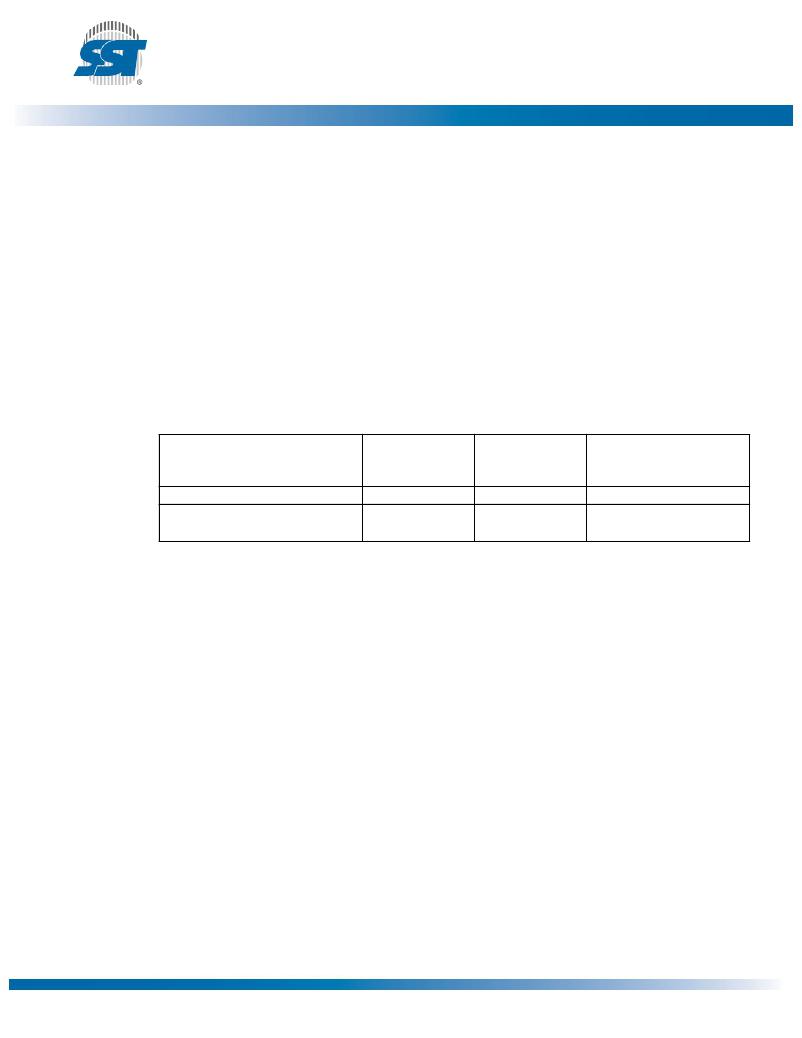
�Product� Identification�
�The� product� identification� mode� identifies� the� device� as� the� SST49LF008A� and� manufacturer� as� SST.�
�Table� 2:� Product� Identification�
�JEDEC� ID�
�Address�
�Byte�
�Data�
�Location�
�Manufacturer’s� ID�
�0000H�
�BFH�
�FFBC0000H�
�Device� ID�
�SST49LF008A�
�0001H�
�5AH�
�FFBC0001H�
�T2.7� 25085�
�Mode� Selection�
�The� SST49LF008A� flash� memory� devices� can� operate� in� two� distinct� interface� modes:� the� Firmware�
�Hub� Interface� (FWH)� mode� and� the� Parallel� Programming� (PP)� mode.� The� IC� (Interface� Configuration�
�pin)� is� used� to� set� the� interface� mode� selection.� If� the� IC� pin� is� set� to� logic� High,� the� device� is� in� PP�
�mode;� while� if� the� IC� pin� is� set� Low,� the� device� is� in� the� FWH� mode.� The� IC� selection� pin� must� be� con-�
�figured� prior� to� device� operation.� The� IC� pin� is� internally� pulled� down� if� the� pin� is� not� connected.� In�
�FWH� mode,� the� device� is� configured� to� interface� with� its� host� using� Intel’s� Firmware� Hub� proprietary�
�protocol.� Communication� between� Host� and� the� SST49LF008A� occurs� via� the� 4-bit� I/O� communication�
�signals,� FWH� [3:0]� and� the� FWH4.� In� PP� mode,� the� device� is� programmed� via� an� 11-bit� address� and�
�an� 8-bit� data� I/O� parallel� signals.� The� address� inputs� are� multiplexed� in� row� and� column� selected� by�
�control� signal� R/C#� pin.� The� column� addresses� are� mapped� to� the� higher� internal� addresses,� and� the�
�row� addresses� are� mapped� to� the� lower� internal� addresses.� See� the� Device� Memory� Map� in� Figure� 5�
�for� address� assignments.�
�?2011� Silicon� Storage� Technology,� Inc.�
�8�
�DS25085A�
�10/11�
�发布紧急采购,3分钟左右您将得到回复。
相关PDF资料
SST49LF016C-33-4C-EIE-T
IC FLASH SER LPC 16MBIT 40TSOP
SST49LF080A-33-4C-WHE-T
IC FLASH SER LPC 8MBIT 32TSOP
SST49LF160C-33-4C-NHE
IC FLASH SER LPC 16MBIT 32PLCC
ST40
DIAC 35-45V BILATERAL TRIG DO214
STRIKER
SURGE SUPPRESSR 120V 7OUT 6'CORD
SUPER-7
SURGE SUPPRESSOR 7 OUT 7' CORD
SUPER6TEL12
SURGE SUPPR 7OUT 12'CORD W/RJ11
SUPER6TEL
SURGE SUPPRESSOR 7OUT W/TEL
相关代理商/技术参数
SST49LF008A-33-4C-NH
制造商:SST 制造商全称:Silicon Storage Technology, Inc 功能描述:2 Mbit / 3 Mbit / 4 Mbit / 8 Mbit Firmware Hub
SST49LF008A-33-4C-NHE
功能描述:闪存 8M (1Mx8) 33MHz Commercial Temp RoHS:否 制造商:ON Semiconductor 数据总线宽度:1 bit 存储类型:Flash 存储容量:2 MB 结构:256 K x 8 定时类型: 接口类型:SPI 访问时间: 电源电压-最大:3.6 V 电源电压-最小:2.3 V 最大工作电流:15 mA 工作温度:- 40 C to + 85 C 安装风格:SMD/SMT 封装 / 箱体: 封装:Reel
SST49LF008A-33-4C-NHE_
制造商:Microchip Technology Inc 功能描述:
SST49LF008A-33-4C-NHE-T
功能描述:闪存 8M (1Mx8) 33MHz 3.0-3.6V Commercial RoHS:否 制造商:ON Semiconductor 数据总线宽度:1 bit 存储类型:Flash 存储容量:2 MB 结构:256 K x 8 定时类型: 接口类型:SPI 访问时间: 电源电压-最大:3.6 V 电源电压-最小:2.3 V 最大工作电流:15 mA 工作温度:- 40 C to + 85 C 安装风格:SMD/SMT 封装 / 箱体: 封装:Reel
SST49LF008A-33-4C-NHE-T-CUT TAPE
制造商:Microchip 功能描述:SST49LF Series 8 Mbit 1024 K x 8 3.3 V Firmware Hub - PLCC-32
SST49LF008A-33-4C-WH
制造商:SST 制造商全称:Silicon Storage Technology, Inc 功能描述:2 Mbit / 3 Mbit / 4 Mbit / 8 Mbit Firmware Hub
SST49LF008A-33-4C-WHE
功能描述:闪存 8 MBIT FIRMWARE HUB RoHS:否 制造商:ON Semiconductor 数据总线宽度:1 bit 存储类型:Flash 存储容量:2 MB 结构:256 K x 8 定时类型: 接口类型:SPI 访问时间: 电源电压-最大:3.6 V 电源电压-最小:2.3 V 最大工作电流:15 mA 工作温度:- 40 C to + 85 C 安装风格:SMD/SMT 封装 / 箱体: 封装:Reel
SST49LF008A-33-4C-WHE_
制造商:Microchip Technology Inc 功能描述: